STM32 Robot Board Pin Mapping Strategy — Migrating from Teensy
Pin mapping strategy and actual layout results from migrating a robot board from Teensy 4.1 to STM32H743.
Robot Board Pin Mapping Strategy
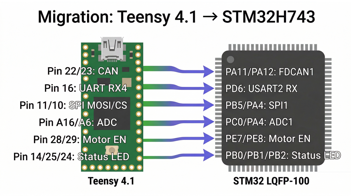 Pin mapping comparison between Teensy 4.1 and STM32H743
7.1 Pin Assignment Principles
- Prevent AF conflicts: Only one AF can be used per pin
- Secure power/ground connections: All 18 power pins on LQFP-100 must be properly connected
- Noise isolation: ADC input pins must be physically separated from high-speed digital signals (CAN, SPI)
- Protect debugger pins: PA13 (SWDIO) and PA14 (SWCLK) must never be repurposed
- Handle unused pins: Set to Analog mode (minimizes current draw) or Output Low
- BOOT0 pin: Connect to GND (normal boot = execute from Flash)
7.2 Teensy → STM32 Pin Mapping Table
Final mapping table from the current Board.h Teensy 4.1 pin configuration to STM32H743VITx:
Communication Peripherals
| Function | Teensy Pin | STM32 Pin | AF | Peripheral | Notes |
|---|---|---|---|---|---|
| CAN TX | 22 | PD1 | AF9 | FDCAN1_TX | Motor CAN bus |
| CAN RX | 23 | PD0 | AF9 | FDCAN1_RX | Motor CAN bus |
| IMU UART RX | 16 (RX4) | PD9 | AF7 | USART3_RX | IMU data receive |
| IMU UART TX | N/C | PD8 | AF7 | USART3_TX | (can double as debug) |
| SPI SCK | (implicit) | PA5 | AF5 | SPI1_SCK | Coms MCU communication |
| SPI MOSI | 11 | PB5 | AF5 | SPI1_MOSI | PA7 reserved for ADC |
| SPI MISO | (implicit) | PB4 | AF5 | SPI1_MISO | PA6 reserved for ADC |
| SPI CS | 10 | PA15 | GPIO | — | Software CS |
| SPI IRQ | 34 | PE0 | GPIO | EXTI0 | Interrupt input |
| SPI RST | 4 | PE1 | GPIO | — | Coms MCU reset |
| Serial TX | 1 | PA9 | AF7 | USART1_TX | (debug/PC communication) |
| Serial RX | 0 | PA10 | AF7 | USART1_RX | (debug/PC communication) |
Analog Inputs (ADC)
| Function | Teensy Pin | STM32 Pin | Channel | Peripheral | Notes |
|---|---|---|---|---|---|
| Torque Sensor Left | A16 | PA0 | IN0 | ADC1 | Load cell L |
| Torque Sensor Right | A6 | PA3 | IN3 | ADC1 | Load cell R (PA3 instead of PA6) |
| Angle Sensor Left | A13 | PC3 | IN13 | ADC1 | Left ankle angle |
| Angle Sensor Right | A12 | PC2 | IN12 | ADC1 | Right ankle angle |
| Maxon Current Left | (maxon_current) | PA1 | IN1 | ADC1 | Left motor current |
| Maxon Current Right | (maxon_current) | PA2 | IN2 | ADC1 | Right motor current |
| (Spare 1) | — | PC4 | IN14 | ADC1 | For expansion |
| (Spare 2) | — | PC5 | IN15 | ADC1 | For expansion |
PWM Outputs
| Function | Teensy Pin | STM32 Pin | AF | Peripheral | Notes |
|---|---|---|---|---|---|
| Maxon PWM Left | (maxon_ctrl_L) | PE9 | AF1 | TIM1_CH1 | Left motor |
| Maxon PWM Right | (maxon_ctrl_R) | PE11 | AF1 | TIM1_CH2 | Right motor |
GPIO Outputs
| Function | Teensy Pin | STM32 Pin | Configuration | Notes |
|---|---|---|---|---|
| Status LED Red | 14 | PB0 | Output PP, Low Speed | RGB LED |
| Status LED Green | 25 | PB1 | Output PP, Low Speed | RGB LED |
| Status LED Blue | 24 | PB2 | Output PP, Low Speed | RGB LED |
| Sync LED | 15 | PB10 | Output PP, Low Speed | Sync LED |
| Motor Stop | 9 | PC6 | Output PP, Pull-Down | Emergency stop |
| Motor Enable L0 | 28 | PD3 | Output PP, Pull-Down | Left joint 0 |
| Motor Enable L1 | 29 | PD4 | Output PP, Pull-Down | Left joint 1 |
| Motor Enable R0 | 8 | PD5 | Output PP, Pull-Down | Right joint 0 |
| Motor Enable R1 | 7 | PD6 | Output PP, Pull-Down | Right joint 1 |
| Sync Default | 5 | PC7 | Output PP | Sync default |
| Speed Check | 33 | PC8 | Output PP | Toggle pin for timing measurement |
GPIO Inputs
| Function | Teensy Pin | STM32 Pin | Configuration | Notes |
|---|---|---|---|---|
| Maxon Error Left | (maxon_err_L) | PE2 | Input, Pull-Up | Error detection (active low) |
| Maxon Error Right | (maxon_err_R) | PE3 | Input, Pull-Up | Error detection (active low) |
System Pins (Do Not Change)
| Function | STM32 Pin | Notes |
|---|---|---|
| SWDIO (Debugger) | PA13 | Never reassign |
| SWCLK (Debugger) | PA14 | Never reassign |
| HSE Crystal IN | PH0 (pin 12) | 8MHz crystal |
| HSE Crystal OUT | PH1 (pin 13) | 8MHz crystal |
| NRST | pin 14 (NRST) | Reset button |
| BOOT0 | pin 94 | Connected to GND (Flash boot) |
7.3 AF Conflict Verification
Key conflict resolutions in the above mapping:
| Issue | Cause | Resolution |
|---|---|---|
| PA6 cannot be used for both ADC and SPI1_MISO | AF conflict | Move SPI1_MISO to PB4 (AF5) |
| PA7 cannot be used for both ADC and SPI1_MOSI | AF conflict | Move SPI1_MOSI to PB5 (AF5) |
| PA1 cannot be used for both ADC (current sensing) and UART4_RX | AF conflict | Move IMU UART to USART3 (PD8/PD9) |
| PA6 used for torque sensor R ADC conflicts with SPI | AF conflict | Move torque sensor R to PA3 (ADC1_IN3) |
7.4 Pin Usage Summary
| Port | Used Pins | Unused Pins | Notes |
|---|---|---|---|
| GPIOA | PA0-5, PA9-10, PA13-15 | PA6-8, PA11-12 | PA11/12 reserved for USB |
| GPIOB | PB0-2, PB4-5, PB10 | PB3, PB6-9, PB11-15 | Plenty of room |
| GPIOC | PC2-8 | PC0-1, PC9-13 | PC13 can be WKUP |
| GPIOD | PD0-1, PD3-6, PD8-9 | PD2, PD7, PD10-15 | Plenty of room |
| GPIOE | PE0-3, PE9, PE11 | PE4-8, PE10, PE12-15 | Plenty of room |
Total pins used: ~40 / Spare pins: ~36 — plenty of room for future expansion
7.5 Pin Map Documentation
The finalized pin mapping should be written to Documentation/Hardware/AR_Walker_STM32_Pinmap.md
using the templates/hardware_pinmap_template.md template.
Previous post: STM32CubeMX Practical Configuration | Next post: STM32 Board Bringup

Henry — Robot Education Founder
Engineer dedicated to democratizing robot education for everyone. From hardware bring-up to AI integration, I document real learning.
Comments
Loading comments...