STM32 Pin System Deep Dive — AF, GPIO Ports, Pin Mapping
Complete guide to STM32 GPIO port naming, LQFP-100 pin mapping, and Alternate Function multiplexer.
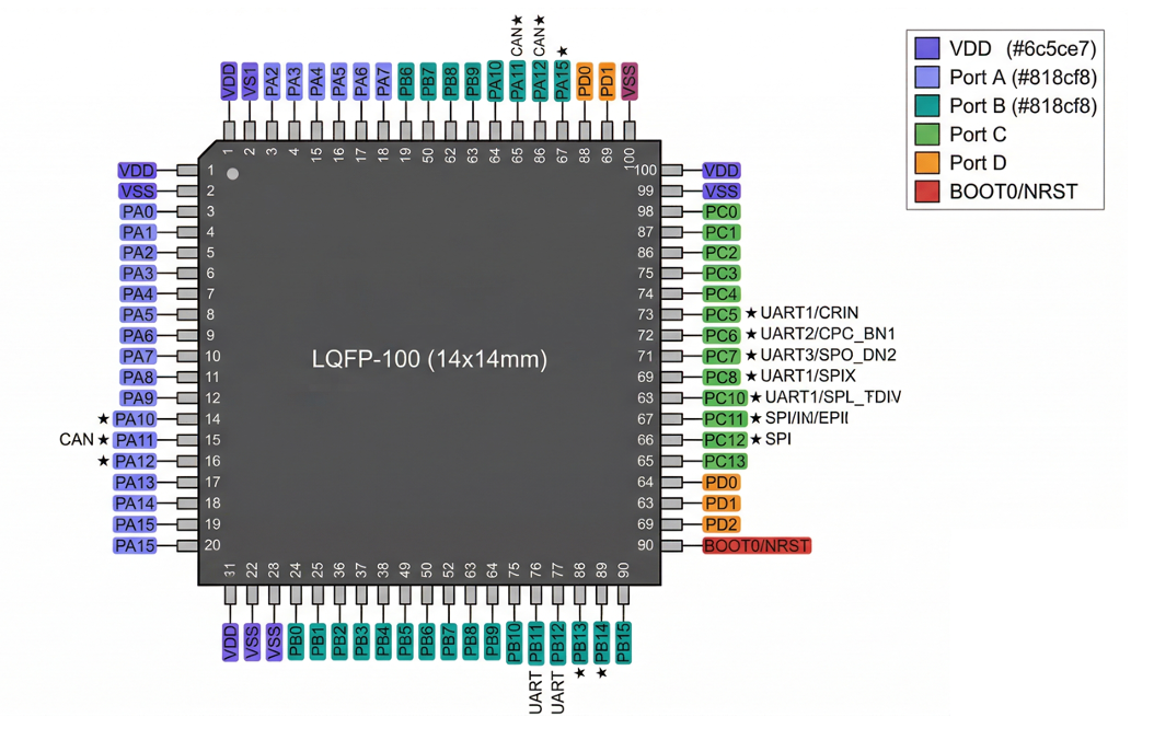 STM32H743VITx LQFP-100 pinout diagram
2.1 Physical Pins vs. GPIO Ports
To understand the STM32 pin system, you need to distinguish between two different "pin numbers":
- Physical pin number: The leg number on the IC package (LQFP-100: pins 1–100)
- GPIO port name: The software name like PA0, PB3, PC13
GPIO port naming convention:
P + [Port letter] + [Pin number]
│    │              │
│    A~K            0~15
│    (port group)   (pin number within group)
GPIO
Examples:
PA0= Port A, Pin 0PB7= Port B, Pin 7PD1= Port D, Pin 1
Available GPIO ports on the STM32H743VITx (LQFP-100):
| Port | Available Pins | Notes |
|---|---|---|
| GPIOA | PA0–PA15 | All 16 pins available |
| GPIOB | PB0–PB15 | All 16 pins available |
| GPIOC | PC0–PC13 | 14 pins (PC14/15 are OSC32) |
| GPIOD | PD0–PD15 | All 16 pins available |
| GPIOE | PE0–PE15 | All 16 pins available |
⚠️ Note: GPIOF–GPIOK are not available on the LQFP-100 package (no physical pins). These ports are only accessible on packages with 144 pins or more.
2.2 LQFP-100 Physical Pin to GPIO Mapping
Mapping between physical pin numbers and GPIO names for the STM32H743VITx (LQFP-100):
                      Pins 76–100 (top)
                ┌──────────────────────┐
                │  76 77 78 ... 99 100 │
        Pins    │                      │  Pins
       51–75    │                      │  1–25
       (right)  │    STM32H743VITx     │  (left)
                │      LQFP-100        │
                │                      │
                │  51 50 49 ... 27 26  │
                └──────────────────────┘
                      Pins 26–50 (bottom)
Key pin mappings (commonly used):
| Physical Pin | GPIO | Main Functions | AF Examples |
|---|---|---|---|
| 14 | PA0 | ADC1_IN0, TIM2_CH1 | AF1(TIM2), AF-(Analog) |
| 15 | PA1 | ADC1_IN1, TIM2_CH2 | AF1(TIM2), AF-(Analog) |
| 16 | PA2 | ADC1_IN2, USART2_TX | AF7(USART2), AF-(Analog) |
| 17 | PA3 | ADC1_IN3, USART2_RX | AF7(USART2), AF-(Analog) |
| 20 | PA4 | ADC1_IN4, SPI1_NSS, DAC1_OUT1 | AF5(SPI1) |
| 21 | PA5 | ADC1_IN5, SPI1_SCK, DAC1_OUT2 | AF5(SPI1) |
| 22 | PA6 | ADC1_IN6, SPI1_MISO, TIM3_CH1 | AF5(SPI1) |
| 23 | PA7 | ADC1_IN7, SPI1_MOSI, TIM3_CH2 | AF5(SPI1) |
| 68 | PA8 | TIM1_CH1, MCO1 | AF1(TIM1), AF0(MCO1) |
| 69 | PA9 | USART1_TX, TIM1_CH2 | AF7(USART1) |
| 70 | PA10 | USART1_RX, TIM1_CH3 | AF7(USART1) |
| 71 | PA11 | USB_OTG_FS_DM, FDCAN1_RX | AF9(FDCAN1) |
| 72 | PA12 | USB_OTG_FS_DP, FDCAN1_TX | AF9(FDCAN1) |
| 76 | PA13 | SWDIO (debugger) | Debug only — do not reassign! |
| 77 | PA14 | SWCLK (debugger) | Debug only — do not reassign! |
| 78 | PA15 | SPI3_NSS, TIM2_CH1 | AF6(SPI3) |
| 35 | PB0 | ADC1_IN8, TIM3_CH3 | AF2(TIM3) |
| 36 | PB1 | ADC1_IN9, TIM3_CH4 | AF2(TIM3) |
| 37 | PB2 | QUADSPI_CLK | AF9(QUADSPI) |
| 89 | PB3 | SPI3_SCK, TIM2_CH2 | AF6(SPI3) |
| 90 | PB4 | SPI3_MISO, TIM3_CH1 | AF6(SPI3) |
| 91 | PB5 | SPI3_MOSI, FDCAN2_RX | AF6(SPI3), AF9(FDCAN2) |
| 92 | PB6 | USART1_TX, FDCAN2_TX, I2C1_SCL | AF7(USART1), AF9(FDCAN2) |
| 93 | PB7 | USART1_RX, I2C1_SDA | AF7(USART1), AF4(I2C1) |
| 95 | PB8 | FDCAN1_RX, I2C1_SCL, TIM4_CH3 | AF9(FDCAN1), AF4(I2C1) |
| 96 | PB9 | FDCAN1_TX, I2C1_SDA, TIM4_CH4 | AF9(FDCAN1), AF4(I2C1) |
| 47 | PB10 | USART3_TX, I2C2_SCL, TIM2_CH3 | AF7(USART3) |
| 48 | PB11 | USART3_RX, I2C2_SDA, TIM2_CH4 | AF7(USART3) |
| 51 | PB12 | SPI2_NSS, USART3_CK | AF5(SPI2) |
| 52 | PB13 | SPI2_SCK, FDCAN2_TX | AF5(SPI2), AF9(FDCAN2) |
| 53 | PB14 | SPI2_MISO, USART3_RTS | AF5(SPI2) |
| 54 | PB15 | SPI2_MOSI, TIM12_CH2 | AF5(SPI2) |
| 8 | PC0 | ADC1_IN10 | AF-(Analog) |
| 9 | PC1 | ADC1_IN11 | AF-(Analog) |
| 10 | PC2 | ADC1_IN12, SPI2_MISO | AF5(SPI2) |
| 11 | PC3 | ADC1_IN13, SPI2_MOSI | AF5(SPI2) |
| 33 | PC4 | ADC1_IN14 | AF-(Analog) |
| 34 | PC5 | ADC1_IN15 | AF-(Analog) |
| 63 | PC6 | USART6_TX, TIM8_CH1 | AF7(USART6) |
| 64 | PC7 | USART6_RX, TIM8_CH2 | AF7(USART6) |
| 65 | PC8 | TIM8_CH3, SDMMC1_D0 | AF3(TIM8) |
| 66 | PC9 | TIM8_CH4, SDMMC1_D1 | AF3(TIM8) |
| 67 | PC10 | USART3_TX, SPI3_SCK | AF7(USART3) |
| 79 | PC11 | USART3_RX, SPI3_MISO | AF7(USART3) |
| 80 | PC12 | SPI3_MOSI, UART5_TX | AF6(SPI3) |
| 7 | PC13 | RTC_TAMP, WKUP | General-purpose GPIO |
| 82 | PD0 | FDCAN1_RX, FMC_D2 | AF9(FDCAN1) |
| 83 | PD1 | FDCAN1_TX, FMC_D3 | AF9(FDCAN1) |
| 84 | PD2 | UART5_RX, TIM3_ETR | AF8(UART5) |
| 85 | PD3 | USART2_CTS, FMC_CLK | AF7(USART2) |
| 86 | PD4 | USART2_RTS, FMC_NOE | AF7(USART2) |
| 87 | PD5 | USART2_TX, FMC_NWE | AF7(USART2) |
| 88 | PD6 | USART2_RX, FMC_NWAIT | AF7(USART2) |
| 55 | PD8 | USART3_TX | AF7(USART3) |
| 56 | PD9 | USART3_RX | AF7(USART3) |
| 100 | PE0 | UART8_RX, TIM4_ETR | AF8(UART8) |
| 1 | PE1 | UART8_TX | AF8(UART8) |
| 2 | PE2 | SPI4_SCK, UART8_TX | AF5(SPI4) |
| 98 | PE9 | TIM1_CH1, FMC_D6 | AF1(TIM1) — for PWM |
| 99 | PE11 | TIM1_CH2, FMC_D8 | AF1(TIM1) — for PWM |
2.3 Pin Function Categories
The 100 pins on the LQFP-100 fall into four broad categories:
| Category | Pins | Count | Description |
|---|---|---|---|
| Power | VDD, VSS, VDDA, VSSA, VREF+, VCAP | ~18 | Power supply (3.3V, GND) |
| Clock | OSC_IN, OSC_OUT (PH0/PH1) | 2 | External crystal connection |
| Reset | NRST | 1 | System reset (active low) |
| Debug | PA13 (SWDIO), PA14 (SWCLK) | 2 | SWD debugger only |
| Boot | BOOT0 | 1 | Boot mode selection |
| GPIO | PA0–PE15 | ~76 | General-purpose I/O + AF |
🔴 Hard rule: PA13/PA14 are the SWD debugger pins. Reassigning them to any other function will make debugging and programming impossible. Always reserve them for SWD.
2.4 Alternate Function (AF) System
One of the most important concepts in STM32. A single GPIO pin can be configured for up to 16 different functions.
AF numbering (AF0–AF15):
| AF Number | Main Functions |
|---|---|
| AF0 | SYS (MCO, SWD, TRACE) |
| AF1 | TIM1, TIM2 |
| AF2 | TIM3, TIM4, TIM5 |
| AF3 | TIM8, TIM15-17 |
| AF4 | I2C1-4 |
| AF5 | SPI1-6 |
| AF6 | SPI2/3, SAI1/2 |
| AF7 | USART1-3, USART6 |
| AF8 | UART4/5, UART7/8, LPUART1 |
| AF9 | FDCAN1/2, QUADSPI, TIM12-14 |
| AF10 | USB OTG, SAI2 |
| AF11 | ETH, UART7 |
| AF12 | FMC, SDMMC, MDIOS |
| AF13 | DCMI, COMP |
| AF14 | LTDC, UART5 |
| AF15 | EVENTOUT |
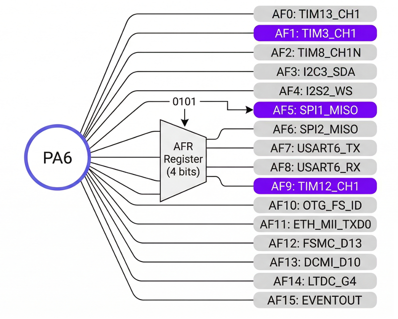 AF0–AF15 multiplexer — select one of 16 functions per pin
AF example — PA7:
PA7 can be assigned any of the following:
- AF0: MCO (microcontroller clock output)
- AF2: TIM3_CH2 (Timer 3 channel 2 = PWM output)
- AF5: SPI1_MOSI (SPI1 master output)
- Analog: ADC1_IN7 (analog input)
Only one AF can be active at a time. If PA7 is configured as SPI1_MOSI, ADC and TIM3 cannot be used on that pin simultaneously.
How to avoid AF conflicts:
- List all the peripherals you need (CAN, UART, SPI, ADC, PWM, etc.)
- Check the pin options for each peripheral (Datasheet Tables 9–12)
- Arrange pins so AFs don't overlap → CubeMX checks for conflicts automatically
2.5 Pin Configuration Registers
Each GPIO pin is controlled through the following registers:
Register          Bits/pin    Function
──────────────────────────────────────────────
GPIOx_MODER      2 bits/pin  Mode selection
                              00 = Input
                              01 = Output
                              10 = Alternate Function
                              11 = Analog

GPIOx_OTYPER     1 bit/pin   Output type
                              0 = Push-Pull
                              1 = Open-Drain

GPIOx_OSPEEDR    2 bits/pin  Output speed
                              00 = Low (up to 12 MHz)
                              01 = Medium (up to 60 MHz)
                              10 = High (up to 85 MHz)
                              11 = Very High (up to 100 MHz)

GPIOx_PUPDR      2 bits/pin  Pull-up/pull-down
                              00 = No Pull
                              01 = Pull-Up
                              10 = Pull-Down
                              11 = Reserved

GPIOx_AFRL       4 bits/pin  AF select (pins 0–7)
GPIOx_AFRH       4 bits/pin  AF select (pins 8–15)
                              0000 = AF0
                              0001 = AF1
                              ...
                              1111 = AF15
Direct register example (configure PA7 as SPI1_MOSI with AF5):
// 1. Enable GPIOA clock
RCC->AHB4ENR |= RCC_AHB4ENR_GPIOAEN;

// 2. Set PA7 to Alternate Function mode
GPIOA->MODER &= ~(0x3 << (7 * 2));     // clear bits
GPIOA->MODER |=  (0x2 << (7 * 2));     // 10 = AF mode

// 3. Select AF5 (SPI1) — PA7 is pin 0–7, so use AFRL
GPIOA->AFR[0] &= ~(0xF << (7 * 4));    // clear bits
GPIOA->AFR[0] |=  (0x5 << (7 * 4));    // AF5 = SPI1

// 4. Push-Pull, Very High Speed
GPIOA->OTYPER &= ~(1 << 7);            // Push-Pull
GPIOA->OSPEEDR |= (0x3 << (7 * 2));    // Very High Speed
In practice you'll use the HAL library, so direct register manipulation is rare. That said, understanding the register layout lets you read register values during debugging and diagnose problems quickly.
2.6 Finding Pin Information in the Datasheet
You need two documents to look up pin information for the STM32H743VITx:
| Document | Contents | What to look for |
|---|---|---|
| Datasheet (DS12110) | Pinout, electrical characteristics, package | Physical pin numbers, AF tables, voltage/current specs |
| Reference Manual (RM0433) | Registers, peripheral operation | GPIO registers, timer config, CAN protocol, etc. |
Key sections to read in the datasheet:
- Tables 9–12: "Alternate function mapping" — full AF0–AF15 mapping for every pin
- Figure 1: LQFP-100 pinout diagram
- Table 7: "Pin definitions" — power/IO type and 5V-tolerance for each pin
💡 Tip: CubeMX lets you browse these tables in a GUI, but getting comfortable reading the datasheet directly pays off significantly when doing hardware design.
Previous post: STM32 Architecture Basics | Next post: STM32 Clock System

Henry — Robot Education Founder
Engineer dedicated to democratizing robot education for everyone. From hardware bring-up to AI integration, I document real learning.
Comments
Loading comments...