STM32 Architecture Basics — Cortex-M7, Memory Map, Bus Architecture
A deep dive into STM32H743VITx's ARM Cortex-M7 core, memory map, and bus architecture.
3 min readby Henry
stm32arm-cortex-m7embedded
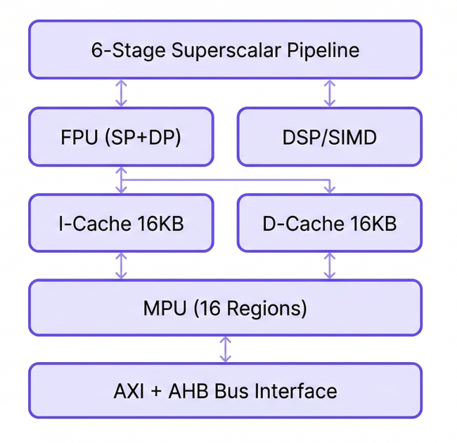 Cortex-M7 core block diagram
1.1 ARM Cortex-M7 Core
The STM32H743VITx is a high-performance microcontroller built around the ARM Cortex-M7 core.
Core Specifications:
| Item | Spec |
|---|---|
| Architecture | ARMv7E-M |
| Pipeline | 6-stage superscalar (dual-issue) |
| FPU | Single-precision (SP) + Double-precision (DP) floating-point |
| DSP | Single-cycle MAC, SIMD instructions |
| I-Cache | 16 KB (instruction cache) |
| D-Cache | 16 KB (data cache) |
| MPU | 16-region Memory Protection Unit |
| Max Clock | 480 MHz |
Why Cortex-M7 for a robot board?
- Reliably drives a 500 Hz control loop (same core as the Teensy 4.1)
- FPU handles PID calculations, torque computations, and other floating-point math in hardware
- DSP instructions accelerate sensor data filtering (IMU, load cells)
- Cache ensures high-speed execution even when running code from Flash
1.2 STM32H743VITx Chip Spec Summary
| Item | Spec | Notes |
|---|---|---|
| Package | LQFP-100 | 100-pin, 14x14mm |
| Flash | 2 MB | Dual-bank |
| Total RAM | 1 MB | See breakdown below |
| ITCM | 64 KB | Instruction-only (0 wait state) |
| DTCM | 128 KB | Fastest RAM (0 wait-state) |
| AXI SRAM | 512 KB | General-purpose, large capacity |
| SRAM1 | 128 KB | D2 domain |
| SRAM2 | 128 KB | D2 domain |
| SRAM3 | 32 KB | D2 domain |
| SRAM4 | 64 KB | D3 domain |
| Backup SRAM | 4 KB | Battery-backed |
| GPIO | Up to 82 | Available on LQFP-100 |
| ADC | 3 (ADC1/2/3) | 16-bit, 3.6 MSPS |
| FDCAN | 2 | CAN FD support |
| UART/USART | 8 | USART1-3,6 + UART4,5,7,8 |
| SPI | 6 | SPI1-6 |
| I2C | 4 | I2C1-4 |
| Timer | Many | TIM1-17 (Advanced, GP, Basic) |
| Operating Voltage | 1.62V – 3.6V | Typically 3.3V |
1.3 Memory Map
In the STM32H7, memory and peripherals are organized by power domain.
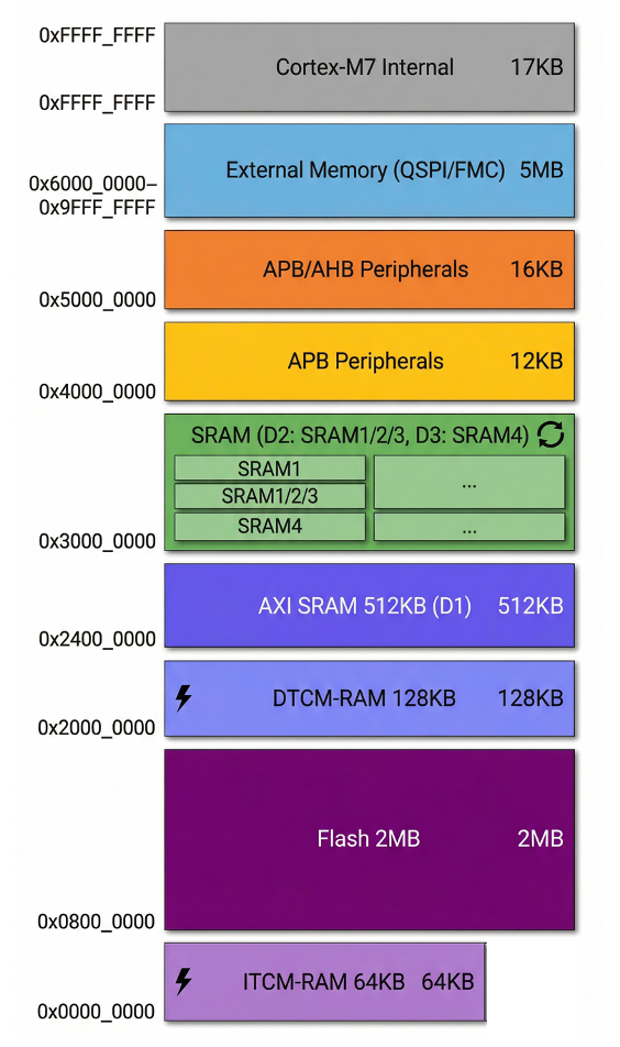 STM32H743 memory map — regions by address
Memory strategy for the robot board:
- DTCM (128 KB): Control loop variables, PID parameters, motor command buffers → fastest access
- AXI SRAM (512 KB): ExoData structs, sensor data arrays, config file parse buffers
- SRAM1/2 (256 KB): DMA transfer buffers (ADC, UART, SPI) → directly accessible by the D2-domain DMA
- SRAM4 (64 KB): Data that must persist through low-power modes
1.4 Bus Architecture
The STM32H7 bus is divided into three power domains (D1, D2, D3):
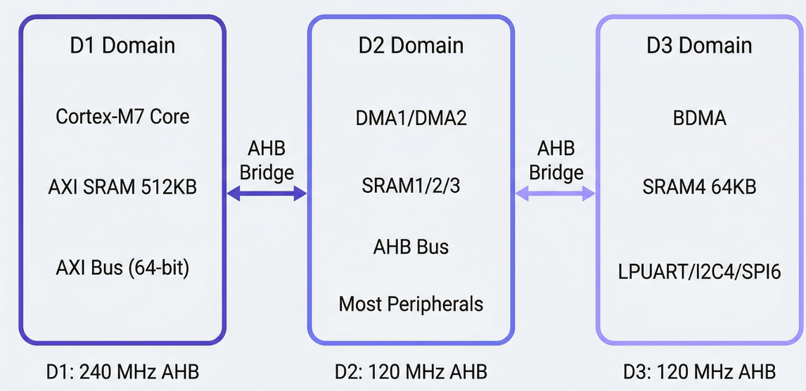 D1/D2/D3 power domains and bus architecture
Key points:
- GPIO is connected to AHB4 (D3 domain), making it accessible from all domains
- FDCAN1/2 sits on APB1 (D2 domain) — when used with DMA1/2, place buffers in SRAM1/2
- ADC1/2 is on APB2 while ADC3 is on AHB4, putting them in different domains — be careful about DMA buffer placement
Next post: STM32 Pin System Deep Dive

Henry — Robot Education Founder
Engineer dedicated to democratizing robot education for everyone. From hardware bring-up to AI integration, I document real learning.
Follow the journey
Comments
Loading comments...